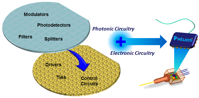
● Optoelectronic 3D integration on silicon
Functional convergence of CMOS electronics with photonics will be attempted through 3D stacking, leading to optoelectronic solutions with small footprint and high-performance. The integrated elements will be receivers, reflective transmitters, arrays of transceivers and a variety of passive optical functionalities in order to proof the viability for exploitation of the endeavoured integration platform. The inclusion of control, supervision and self-calibration mechanisms at the electrical layer offers the unique advantage to provide intelligent and robust optoelectronic systems on a single chip. This functional convergence of photonics and electronics will be achieved by means of 3D integration based on wafer bonding techniques in combination with through-silicon via technology. CMOS-compatible processes guarantee cost-efficiency, high functionality and high reliability for the produced optoelectronic chips.
● A new class of through-silicon vias and local interconnect technology for on-chip RF signal transmission
A new type of through-silicon vias will be developed, aiming at vertical signal propagation through the 3D optoelectronic chip structure at high frequencies at 10 GHz. Novel designs for the TSVs, novel “local interconnects” and improved fabrication processes will be employed in order to push down parasitic capacitance and resistance for high-speed on-chip signal propagation paths.
● Crosstalk-robust co-integration of chip elements with unbalanced signal levels
PHELICITI will pursue the robust co-integration of receiving and transmitting optoelectronics featuring highly unbalanced optical and electrical power levels among up to 8 communication channels. Cross-talk robust designs will be achieved through an optimised silicon interposer technology and at the level of component and system design.